PDF Publication Title:
Text from PDF Page: 021
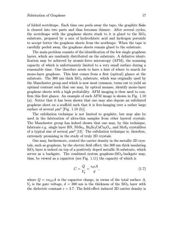
Fabrication of Graphene 17 of folded scotchtape. Each time one peels away the tape, the graphite flake is cleaved into two parts and thus becomes thinner. After several cycles, the scotchtape with the graphene sheets stuck to it is glued to the SiO2 substrate, prepared by a mix of hydrochloric acid and hydrogen peroxide to accept better the graphene sheets from the scothtape. When the tape is carefully peeled away, the graphene sheets remain glued to the substrate. The main problem consists of the identification of the few single graphene layers, which are randomly distributed on the substrate. A definitve identi- fication may be achieved by atomic-force microscopy (AFM), the scanning capacity of which is unfortunately limited to a very small surface during a reasonable time. One therefore needs to have a hint of where to search for mono-layer graphene. This hint comes from a first (optical) glance at the substrate. The 300 nm thick SiO2 substrate, which was originally used by the Manchester group and which is now most common, turns out to yield an optimal contrast such that one may, by optical meanse, identify mono-layer graphene sheets with a high probability. AFM imaging is then used to con- firm this first glance. An example of such AFM image is shown in Fig. 1.10 (a). Notice that it has been shown that one may also depose an exfoliated graphene sheet on a scaffold such that it is free-hanging over a rather large surface of several μm2 [Fig. 1.10 (b)]. The exfoliation technique is not limited to graphite, but may also be used in the fabrication of ultra-thin samples from other layered crystals. The Manchester group has indeed shown that one may, by this technique, fabricate e.g. single layer BN, NbSe2, Bi2Sr2CaCu2Ox, and MoS2 crystallites of a typical size of several μm2 [13]. The exfoliation technique is, therefore, extremely promising in the study of truly 2D crystals. One may, furthermore, control the carrier density in the metallic 2D crys- tals, such as graphene, by the electric field effect; the 300 nm thick insulating SiO2 layer is indeed on top of a positively doped metallic Si substrate, which serves as a backgate. The combined system graphene-SiO2-backgate may, thus, be viewed as a capacitor (see Fig. 1.11) the capacity of which is C = Q = ǫ0ǫA, (1.7) Vg d where Q = en2DA is the capacitor charge, in terms of the total surface A, Vg is the gate voltage, d = 300 nm is the thickness of the SiO2 layer with the dielectric constant ǫ = 3.7. The field-effect induced 2D carrier density isPDF Image | Physical Properties of Graphene
PDF Search Title:
Physical Properties of GrapheneOriginal File Name Searched:
CoursGraphene2008.pdfDIY PDF Search: Google It | Yahoo | Bing
Salgenx Redox Flow Battery Technology: Power up your energy storage game with Salgenx Salt Water Battery. With its advanced technology, the flow battery provides reliable, scalable, and sustainable energy storage for utility-scale projects. Upgrade to a Salgenx flow battery today and take control of your energy future.
| CONTACT TEL: 608-238-6001 Email: greg@infinityturbine.com | RSS | AMP |