PDF Publication Title:
Text from PDF Page: 011
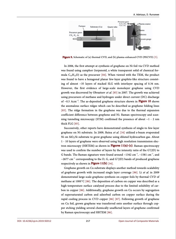
A. Adetayo, D. Runsewe Figure 9. Schematic of (a) thermal CVD, and (b) plasma-enhanced CVD (PECVD) [5]. In 2006, the first attempt at synthesis of graphene on Ni foil via CVD method was found using camphor (terpenoid, a white transparent solid of chemical for- mula C10H16O) as the precursor [84]. When viewed with the TEM, the product was found to have a hexagonal planar few-layer graphite-like structure consist- ing of almost ~35 layers of stacked SLG with interlayer spacing of 0.34 nm. However, the first evidence of large-scale monolayer graphene using CVD growth was discovered by Obraztsov et al. [85] in 2007. The growth was achieved using precursors of methane and hydrogen under direct current (DC) discharge of ~0.5 Acm−2. The as-deposited graphene structure shown in Figure 10 shows the anomalous surface ridges which can be described as graphene folding lines [85]. The ridge formation in the graphene was due to the thermal expansion coefficient difference between graphene and Ni. Raman spectroscopy and scan- ning tunneling microscopy (STM) confirmed the presence of about ~1 - 2 nm thick FLG [85]. Successively, other reports have demonstrated synthesis of single-to few-layer graphene on Ni substrate. In 2009, Reina et al. [34] utilized e-beam evaporated Ni on SiO2/Si substrate to grow graphene using diluted hydrocarbon gas. About 1 - 10 layers of graphene were observed using high resolution transmission elec- tron microscopy (HRTEM) as shown in Figures 11(a)-(c). Raman spectroscopy was used to confirm the number of layers by the intensity ratio of the G’(2D) to G bands. The Raman signature were found around ~1342 cm−1, ~1581 cm−1, and ~2677 cm−1 corresponding to the D, G, and G’(2D) bands of produced graphene respectively as shown in Figure 11(b) [34]. Graphene growth on Cu substrate displays another method towards scalability of graphene growth with increased single layer coverage [86]. Li et al. in 2009 demonstrated large-scale graphene synthesis on copper foils by thermal CVD of methane at 1000 ̊C [86]. The deposition of carbon on copper was described as a high-temperature surface catalyzed process due to the limited solubility of car- bon in copper [86]. Additionally, graphene growth on Cu occurs by segregation of supersaturated carbon and adsorbed carbon on copper surface during the rapid cooling process in CVD copper [86] [87]. Following growth of graphene on Cu foil, grown graphene was transferred onto another surface through cop- per etching yielding several chemically unaffected layers of graphene confirmed by Raman spectroscopy and HRTEM [86]. DOI: 10.4236/ojcm.2019.92012 217 Open Journal of Composite MaterialsPDF Image | Synthesis and Fabrication of Graphene and Graphene Oxide
PDF Search Title:
Synthesis and Fabrication of Graphene and Graphene OxideOriginal File Name Searched:
OJCM-2019042814574897.pdfDIY PDF Search: Google It | Yahoo | Bing
Salgenx Redox Flow Battery Technology: Power up your energy storage game with Salgenx Salt Water Battery. With its advanced technology, the flow battery provides reliable, scalable, and sustainable energy storage for utility-scale projects. Upgrade to a Salgenx flow battery today and take control of your energy future.
CONTACT TEL: 608-238-6001 Email: greg@infinityturbine.com (Standard Web Page)