PDF Publication Title:
Text from PDF Page: 003
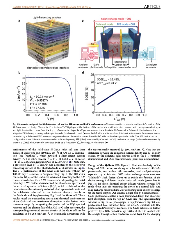
NATURE COMMUNICATIONS | https://doi.org/10.1038/s41467-020-20287-w ARTICLE Fig. 1 Schematic design of the SJ-GaAs solar cell and the SFB device and its PV performance. a The cross-section schematic and layer information of the SJ-GaAs solar cell design. The contact/protection (Ti/TiO2) layer at the bottom of the device stack will be in direct contact with the aqueous electrolyte and light illumination comes from the top n+-GaAs contact layer. b J–V performance of the solid-state SJ-GaAs cell. c Schematic illustration of the integrated SFB device, showing a GaAs photoanode (as shown in panel (a)) on the left side and two carbon felts inert in two electrolyte compartments separated by a Selemion DSV anion exchange membrane. Illumination comes from the left side to the GaAs photoelectrode. The SFB device can be configured to three different operation modes: solar cell (green), RFB (blue) monitored by Channel 1 (CH1), and solar recharge (red) mode monitored by channel 2 (CH2). d Numerically calculated SOEE as a function of E0cell by using J–V data from (b). performance of the solid-state SJ-GaAs solar cell was then evaluated under one sun (100 mW cm−2) of AM 1.5 G illumina- tion (see “Methods”), which revealed a short-circuit current density (JSC) of 30.73 mA cm−2, a VOC of 0.958 V, a fill-factor (FF) of 77.32% and a resulting PCE of 22.78% (Fig. 1b). Note that, a protection layer of Ti/TiO2/Pt was deposited on the electrolyte contacting surface of the photoelectrode as illustrated in Fig.1a. The J–V performance of the GaAs cells with and without Ti/ TiO2/Pt layer is shown in Supplementary Fig. 1. The DC series resistance (RDC) of the GaAs cell calculated according to the J–V curve showed a less than 0.3% increase after depositing the metal oxide layer. We further characterized the absorbance spectra and the external quantum efficiency (EQE, which is defined as the ratio between the externally collected photo-generated carriers of the solid-state solar cell to the incident photons, details in the Methods and Supplementary Fig. 2) of the GaAs cell. These results reveal the outstanding optical and electrical performances of the GaAs cell and maximum absorption in the desired solar spectrum range. By integrating the product of the EQE spectral response and the photon flux of the AM 1.5 G solar spectrum, the corresponding converted current density of the GaAs cell can be calculated to be 26.65 mA cm−2, in reasonable agreement with the experimentally measured JSC (30.73 mA cm−2). Note that the difference between the converted current density and JSC is likely caused by the different light sources used in the J–V (uniform illumination) and EQE measurements (point-like illumination). Design of the SJ-GaAs SFB. Figure 1c illustrates the design of the integrated SFB device, consisting of a back-illuminated SJ-GaAs photoanode, two carbon felt electrodes, and anolyte/catholyte separated by a Selemion DSV anion exchange membrane (see “Methods”). Such design allows us to switch the function of the device among 3 different modes: solar cell mode (green line in Fig. 1c), for direct electrical energy delivery without storage; RFB mode (blue line), for operating the device as a normal RFB; and solar recharge mode (red line), for converting solar energy to charge up the redox couples. Our unusual design of n–p–n sandwiched SJ- GaAs photoanode enables a back-illuminated design that allows for light absorption from the top n+-GaAs side (the light-harvesting window in Fig. 1a, see photograph in Supplementary Fig. 3a), and photoexcited hole extraction from the n-GaAs substrate side (the photoelectrode/electrolyte interface). The GaAs substrate is further protected by a TiO2 protection layer (80 nm), then in contact with the anolyte through a thin conductive metal layer for the charging NATURE COMMUNICATIONS | (2021)12:156 | https://doi.org/10.1038/s41467-020-20287-w | www.nature.com/naturecommunications 3PDF Image | flow battery enabled single-junction GaAs photoelectrode
PDF Search Title:
flow battery enabled single-junction GaAs photoelectrodeOriginal File Name Searched:
s41467-020-20287-w.pdfDIY PDF Search: Google It | Yahoo | Bing
Salgenx Redox Flow Battery Technology: Salt water flow battery technology with low cost and great energy density that can be used for power storage and thermal storage. Let us de-risk your production using our license. Our aqueous flow battery is less cost than Tesla Megapack and available faster. Redox flow battery. No membrane needed like with Vanadium, or Bromine. Salgenx flow battery
| CONTACT TEL: 608-238-6001 Email: greg@salgenx.com | RSS | AMP |